UNIDENTIFIED
786 ACIO VESA MOTHERBOARD
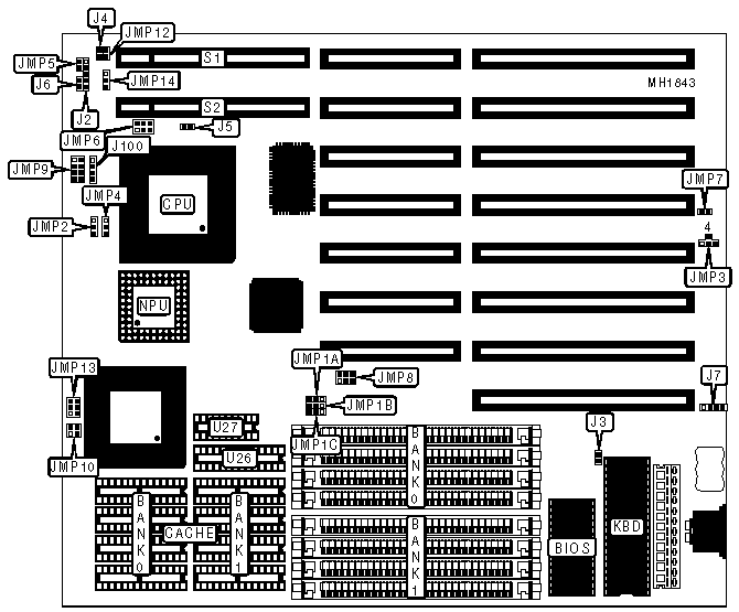
|
Processor |
80386DX/CX486DLC/80486SX/80486DX/80486DX2 |
|
Processor Speed |
25/33/40/50(internal)/50/66(internal)MHz |
|
Chip Set |
Unknown |
|
Max. Onboard DRAM |
32MB |
|
Cache |
64/128/256KB |
|
BIOS |
Unknown |
|
Dimensions |
254mm x 218mm |
|
I/O Options |
32-bit VESA local bus slots (2) |
|
NPU Options |
80387DX |
|
CONNECTIONS | |||
|
Purpose |
Location |
Purpose |
Location |
|
Power LED & keylock |
J2 |
External battery |
J7 |
|
Turbo switch |
J4 |
Speaker |
J100 |
|
Turbo LED |
J5 |
32-bit VESA Local bus slot |
S1 |
|
Reset switch |
J6 |
32-bit VESA Local bus slot |
S2 |
|
USER CONFIGURABLE SETTINGS | |||
|
Function |
Jumper |
Position | |
|
� |
Monitor type select color |
J3 |
Closed |
|
Monitor type select monochrome |
J3 |
Open | |
|
� |
CMOS memory normal operation (Internal battery) |
JMP3 |
pins 2 & 3 closed |
|
� |
CMOS memory normal operation (External battery) |
JMP3 |
pins 1 & 2 closed |
|
CMOS memory clear |
JMP3 |
pins 2 & 4 closed | |
|
� |
NPU enabled |
JMP4 |
pins 1 & 2 closed |
|
NPU disabled |
JMP4 |
pins 2 & 3 closed | |
|
� |
Factory configured - do not alter |
JMP6 |
pins 1 & 4 closed |
|
� |
VESA local bus enabled |
JMP10 |
Open |
|
VESA local bus disabled |
JMP10 |
Closed | |
|
DRAM CONFIGURATION | ||
|
Size |
Bank 0 |
Bank 1 |
|
1MB |
(4) 256K x 9 |
NONE |
|
2MB |
(4) 256K x 9 |
(4) 256K x 9 |
|
4MB |
(4) 1M x 9 |
NONE |
|
5MB |
(4) 1M x 9 |
(4) 256K x 9 |
|
8MB |
(4) 1M x 9 |
(4) 1M x 9 |
|
16MB |
(4) 4M x 9 |
NONE |
|
32MB |
(4) 4M x 9 |
(4) 4M x 9 |
|
Note:The exact locations of Bank 0 & Bank 1 is unknown. | ||
|
CACHE CONFIGURATION | ||||
|
Size |
Bank 0 |
Bank 1 |
TAG/U26 |
TAG/U27 |
|
64KB |
(4) 8K x 8 |
(4) 8K x 8 |
(1) 8K x 8 |
(1) 8K x 8 |
|
128KB |
(4) 32K x 8 |
NONE |
(1) 8K x 8 |
(1) 8K x 8 |
|
256KB |
(4) 32K x 8 |
(4) 32K x 8 |
(1) 32K x 8 |
(1) 32K x 8 |
|
Note:The exact locations of Bank 0 & Bank 1 is unknown. | ||||
|
CACHE JUMPER CONFIGURATION | ||||
|
Size |
JMP1A |
JMP1B |
JMP1C |
JMP8 |
|
64KB |
pins 1 & 2 closed |
pins 1 & 2 closed |
pins 1 & 2 closed |
pins 1 & 2 and 4 & 5 |
|
128KB |
pins 2 & 3 closed |
pins 1 & 2 closed |
pins 2 & 3 closed |
pins 2 & 3 and 4 & 5 |
|
256KB |
pins 2 & 3 closed |
pins 2 & 3 closed |
pins 2 & 3 closed |
pins 2 & 3 and 5 & 6 |
|
Note:Pins designated should be in the closed position. The exact locations of Banks 0 & Bank 1 is unknown. | ||||
|
CPU TYPE CONFIGURATION | |||||
|
Type |
JMP2 |
JMP5 |
JMP7 |
JMP12 |
JMP13 |
|
80386DX |
Open |
Closed |
Open |
Open |
pins 2 & 3 and 5 & 6 |
|
CX486DLC |
Open |
Open |
Closed |
Closed |
pins 1 & 2 and 4 & 5 |
|
80486SX |
pins 1 & 2 closed |
Open |
Closed |
Closed |
pins 1 & 2 and 4 & 5 |
|
80486DX |
pins 2 & 3 closed |
Open |
Closed |
Closed |
pins 1 & 2 and 4 & 5 |
|
80486DX2 |
pins 2 & 3 closed |
Open |
Closed |
Closed |
pins 1 & 2 and 4 & 5 |
|
Note:Pins designated should be in the closed position. | |||||
|
CPU SPEED CONFIGURATION | ||
|
Speed |
JMP9 |
JMP14 |
|
80386DX/25MHz |
pins 1 & 5 and 2 & 6 closed |
pins 1 & 2 closed |
|
80386DX/33MHz |
pins 1 & 5 and 4 & 8 closed |
pins 1 & 2 closed |
|
80386DX/40MHz |
1 & 5, 3 & 7 and 4 & 8 closed |
pins 1 & 2 closed |
|
80486SX/50MHz |
pins 3 & 7 closed |
pins 2 & 3 closed |
|
80486DX/25MHz |
pins 2 & 6 closed |
pins 1 & 2 closed |
|
80486DX/33MHz |
pins 4 & 8 closed |
pins 1 & 2 closed |
|
80486DX2/50i MHz |
pins 2 & 6 closed |
pins 2 & 3 closed |
|
80486DX2/66i MHz |
pins 4 & 8 closed |
pins 1 & 2 closed |